Crystal Diffraction (Diffraction Simulator)
Crystal Diffraction simulates single-crystal X-ray and electron diffraction patterns.
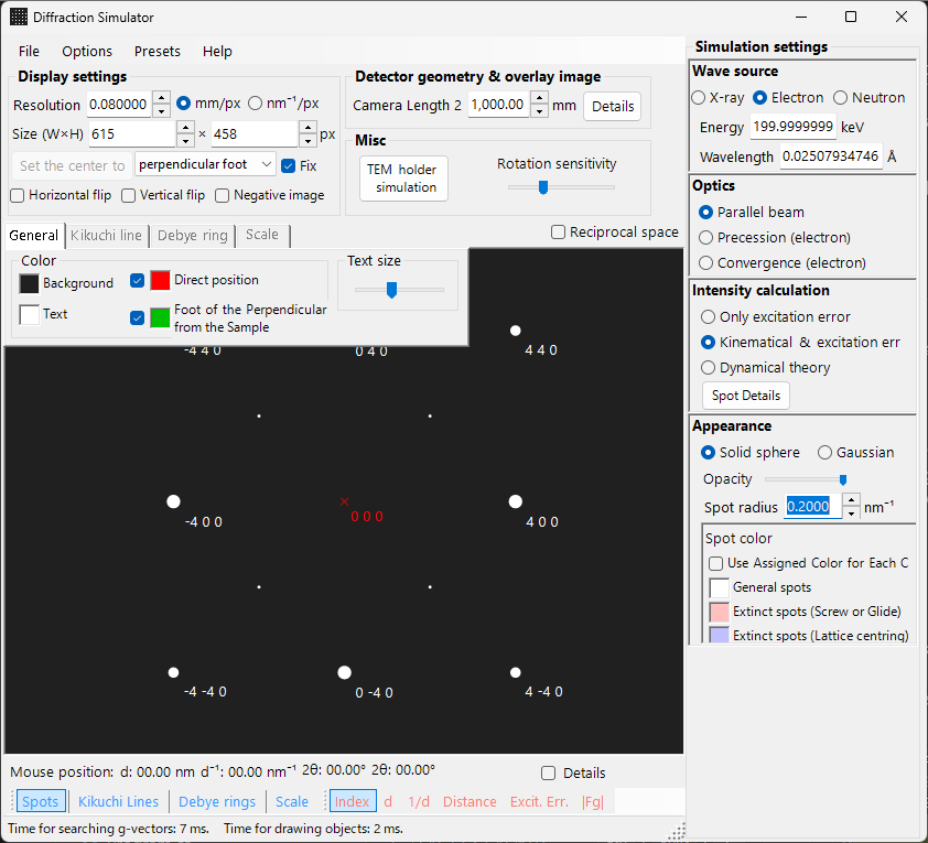
Main area
| Operation | Action |
|---|---|
| Left drag | Rotate |
| Centre drag | Translate |
| Right drag | Zoom in |
| Right click | Zoom out |
| Left double-click | Spot details |
File menu
Preset
Toolbar

Spots, Kikuchi Lines, Debye rings, Scale, label options (Index / d / Distance / Excit. Err. / |Fg|).
Display settings / Detector geometry
Display settings
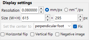
Resolution, image Size (W×H), Set the center to / Fix, and Horizontal flip / Vertical flip / Negative image of the pattern. Tick Reciprocal space to draw the Ewald sphere and reciprocal-lattice vectors.
Misc
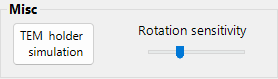
Includes the rotation-sensitivity slider and the TEM holder simulation button (see below).
TEM holder simulation
Opens a window that links the diffraction pattern to a double-tilt (or rotation) TEM holder: set the holder tilt angles and the pattern/orientation updates accordingly, and the reachable orientations can be shown on a stereonet. Added in v4.914.
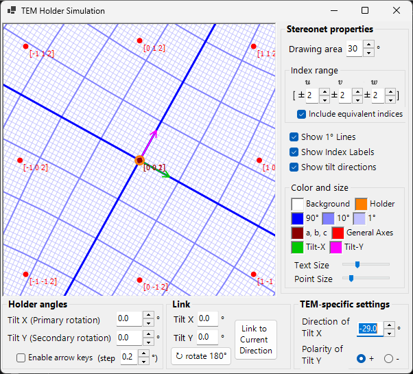
The stereonet (left) plots crystal axes/zone axes with the holder's tilt directions (Tilt-X, Tilt-Y arrows). Set the primary/secondary tilt angles under Holder angles; Link to Current Direction couples the holder to the current crystal orientation, and the TEM-specific settings define each tilt axis direction and polarity for your instrument.
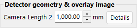
Detector geometry & overlay image
Tab menu
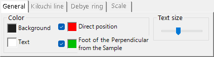
General
Kikuchi lines
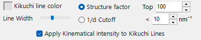
Toggle from the toolbar; choose the reflections by Structure factor (Top N) or 1/d Cutoff, and set the line width and colour.
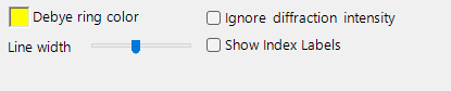
Debye rings
Scale
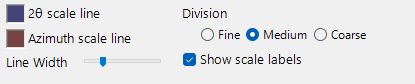
Spot property
Wave Length
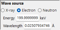
X-ray (characteristic/synchrotron), Electron, Neutron. Set energy or wavelength.
Incident beam mode
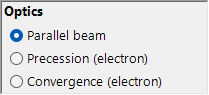
Parallel beam, Precession (electron) (PED), Convergence (electron) (CBED)
Intensity calculation
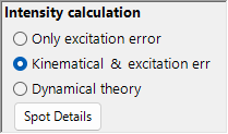
- Only excitation error
- Kinematical & excitation error
- Dynamical theory (Bloch wave, electron only)
Appearance
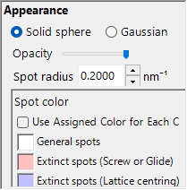
Solid sphere or Gaussian. Opacity, radius, brightness, colour scale.
Bloch wave parameters
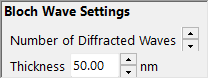
Number of Diffracted Waves and Thickness.
PED parameters
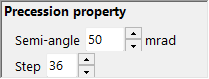
Semi-angle and step.
Detector geometry (detailed)
Detector geometry settings

Detector area and overlapped image
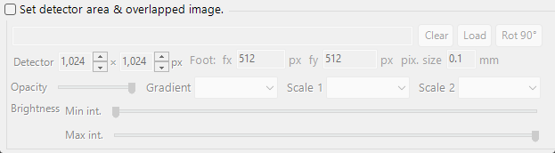
See Appendix A2. Detector Coordinate System.
Diffraction spot information
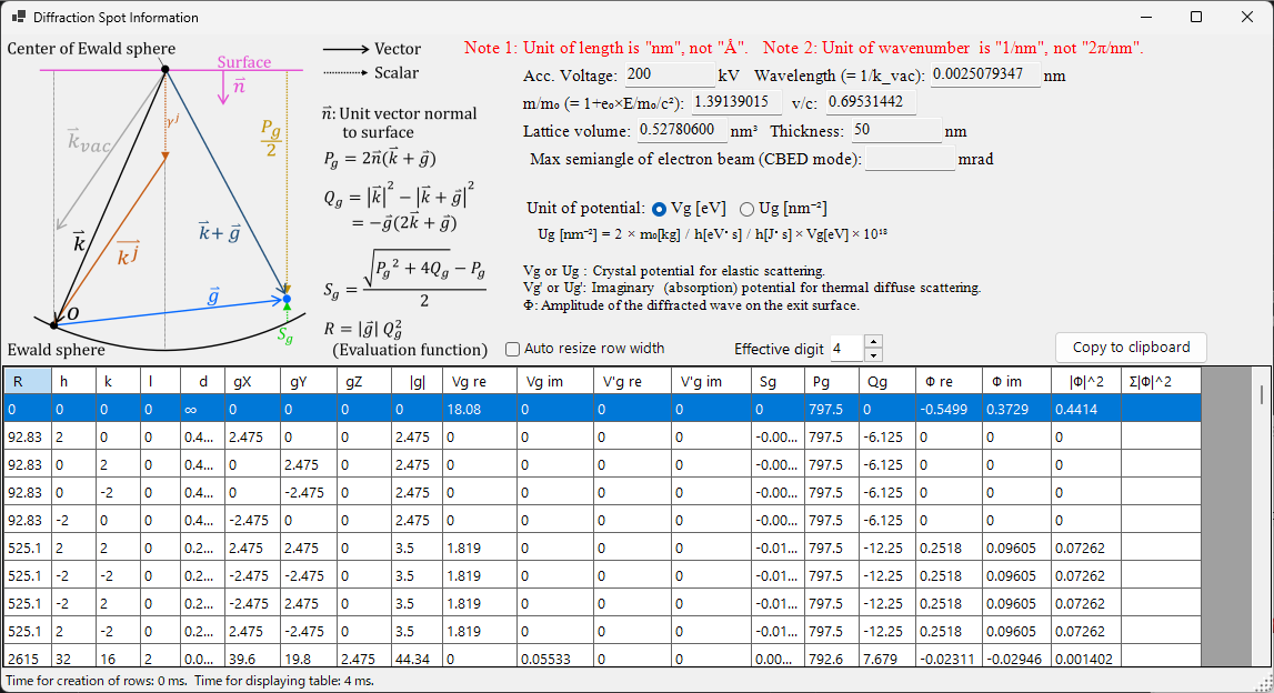
Lists the per-reflection details computed by the Bethe dynamical theory (Bloch-wave method). Open it with the Spot Details button (intensity-calculation panel) or the Details check box.
Schematic and definitions
The schematic (top left) shows the vectors on the Ewald sphere and defines the quantities used in the table (n̂ is the unit vector normal to the sample surface, k is the incident wavevector, g is the reciprocal-lattice vector).
- P_g = 2 n̂·(k + g)
- Q_g = |k|² − |k + g|² = −g·(2k + g)
- Excitation error S_g = ( √(P_g² + 4Q_g) − P_g ) / 2
- Evaluation function R = |g|·Q_g² — ranks reflections by how strongly they are excited (smaller = closer to the Ewald sphere = more strongly excited; the transmitted beam g=0 has R=0 and comes first). The table is sorted by ascending R.
Table columns
| Column | Meaning |
|---|---|
| R | evaluation function R = |g|·Q_g² (above; used for selecting/ordering reflections) |
| h, k, (i,) l | Miller indices (i is the redundant hexagonal index, shown only for hexagonal crystals) |
| d | interplanar spacing (nm) |
| gX, gY, gZ | components of the reciprocal-lattice vector g (1/nm) |
| |g| | magnitude of g (1/nm) |
| Vg re / Vg im | Fourier coefficient of the crystal potential for elastic scattering, V_g (real / imaginary) |
| V'g re / V'g im | imaginary (absorption) potential for thermal diffuse scattering, V'_g (real / imaginary) |
| Sg | excitation error S_g (above; 1/nm) |
| Pg | auxiliary quantity P_g = 2 n̂·(k+g) (above) |
| Qg | auxiliary quantity Q_g = −g·(2k+g) (above) |
| Φ re / Φ im | complex amplitude Φ of the dynamical diffracted wave on the exit surface (real / imaginary) |
| |Φ|^2 | diffracted intensity |Φ|² of that reflection |
| Σ|Φ|^2 | cumulative sum of |Φ|² (total over reflections; useful as an intensity-conservation check) |
Potential units and other controls
- Unit of potential — switches the displayed potential between Vg [eV] (electrostatic potential, eV) and Ug [nm⁻²] (the scaled quantity U_g = 2m₀/h² · V_g that enters the Bloch-wave equations). The column headers change accordingly between Vg / V'g and Ug / U'g.
- Above the table, the accelerating voltage, wavelength (= 1/k_vac), relativistic mass ratio m/m₀, speed ratio v/c, lattice volume, sample thickness, and (in CBED mode) the maximum semi-angle of the electron beam are shown.
- Note 1: the unit of length is nm, not Å. Note 2: the unit of wavenumber is 1/nm, not 2π/nm.
- Effective digit — number of significant digits shown. Auto resize row width — auto-fit column widths. Copy to clipboard — exports the table as text that can be pasted into a spreadsheet.