CBED Simulation
CBED (Convergent-Beam Electron Diffraction) simulation computes and displays convergent-beam diffraction patterns using the Bloch wave (Bethe) method. CBED patterns show diffraction disks instead of spots and contain rich information about crystal symmetry, thickness, and structure.
This page lists all settings of the dedicated window that opens when you select Wavelength = Electron and Incident beam = Convergence (CBED, electron only) in the Diffraction Simulator. Switching the incident beam to convergence automatically switches Intensity calculation to Dynamical, and this CBED settings window opens. For drawing and saving diffraction patterns and other operations common to the diffraction simulator, see the overview page.
GUI conditions: Wave Length = Electron · Incident beam = Convergence (CBED, electron only) · Intensity calculation = Dynamical (automatic)
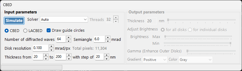
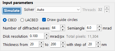
Input parameters
| Parameter | Description | Default / Typical |
|---|---|---|
| Mode | CBED: standard convergent-beam pattern where each disk corresponds to one reflection, with the transmitted disk (000) at the center. LACBED (Large-Angle CBED): large-angle convergent-beam pattern where disks from different reflections overlap. Useful for observing higher-order Laue zone (HOLZ) lines and symmetry | CBED |
| Convergence semi-angle (mrad) | Half-angle of the convergent beam cone. Determines the size of each diffraction disk (the disk diameter in reciprocal space corresponds to \(2\alpha\)) | 5–30 mrad |
| Disk resolution (mrad/px) | Angular resolution within each disk. Smaller values give higher resolution, but the number of beam directions (pixels) computed grows as the square, so the computation time also increases quadratically. The resulting total pixel count (= total number of beam directions) is shown to the right | — |
| No. of Bloch waves | Maximum number of beams included in the Bloch wave calculation at each incident beam direction. More beams give higher accuracy, but the cost of the eigenvalue problem grows as \(O(N^3)\) | 100–500 |
| Thickness range | Start, end, and step values of the sample thickness (nm). Multiple thicknesses are computed together and switched with the thickness slider on the output side | — |
| Solver | Calculation engine for the eigenvalue problem. Auto: automatically selects the best solver. Eigenproblem (MKL): Intel MKL based (fastest). Eigenproblem (Eigen): Eigen C++ library. Managed: pure .NET managed (slowest but always available) | Auto |
| Thread count | Number of parallel threads for the calculation | — |
| Draw disk outlines | When checked, draws a circle indicating the boundary of each diffraction disk | — |
Run / Stop
- Start : starts the CBED simulation with the current input parameters.
- Stop : cancels the running calculation.
Output parameters
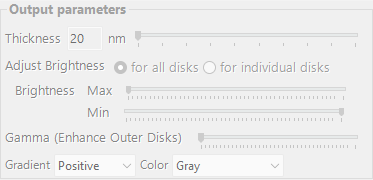
Once the calculation completes, the output parameters become available. All of them change only the display without recomputing.
| Parameter | Description |
|---|---|
| Sample thickness | Selects the sample thickness to display, within the thickness range of the input parameters, using a slider |
| Brightness adjustment | Common to all disks: uses a common brightness scale across all disks to display the complete CBED pattern. Per disk: displays a single selected disk at full resolution, normalized within that disk |
| Brightness (Max / Min) | Upper and lower limits of the displayed intensity. Adjust when you want to emphasize weak features |
| γ (emphasis of outer disks) | Gamma correction. Used to make the dark outer high-angle disks easier to see relative to the central transmitted disk |
| Scale | Selects the intensity gradation from Positive / Negative (black-white inverted) |
| Color | Color map used for display. Choose from Gray and others |
Physical background
In CBED, the incident beam is regarded as a cone of plane waves with different directions. For each direction (each point within the convergence aperture = a partial incident plane wave), the Bloch wave method solves the electron Schrödinger equation inside the crystal, and the results are rearranged as diffraction disks. HOLZ (higher-order Laue zone) lines appear as fine dark/bright lines within the disks, arising from reflections in upper Laue zones. They are sensitive to the lattice parameter along the \(c\) axis and are useful for three-dimensional structure analysis.
For the theoretical details, see CBED calculation.